PCB Design Guidelines
PCB layout is a big domain filled with mysteries. Many big companies have SI experts to help with the design process, guiding the PCB layout engineer away from EMI harm. For the rest of us mortal humans, there are general guidelines for PCB layout that we follow in our designs. Below are some points that will help in making the design more robust and manufacture friendly.
General Notes:
The PCB design should not only be about connecting the pads together. This is the end goal, but reaching this goal should be done following guideline instructions.
- Professional PCB designs are almost always aesthetically pleasing. This is not to be taken slightly when designing a PCB. The design should be clean and neat.
- No matter how good you are in PCB design, there is always room for enhancements. That is why design review is a must every-time. The reviewer shouldn’t necessarily have a bigger experience, actually reviewing someone else’s work is a great way to gain experience.
- Contrary to popular belief, sharp right angle corners on tracks don’t produce measurable EMI or other problems. Nevertheless, tracks should only have 45 degrees angles. Avoid the use of right angles, and under no circumstances use an angle greater than 90 degrees. The reason is because these angles just don’t look good and they might cause manufacturing problems.
Zoning and Placing:
A good component placement will yield a good PCB layout. Defining the general location of all the components on the blank PCB should be done before drawing any trace. Since this is not enough, zoning should take care of grouping together components that have similar functionalities. The figure below from the TI PCB Design Guidelines For Reduced EMI shows a good component placement.
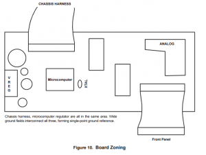
As we can see from the image, high speed logic including the microcontroller are placed next to the power supply. As we move away we start placing slower components. And at the far end we have the analog components. This will keep the analog signals clean, grouped and isolated from any interference caused by the digital signal.
Zoning and placing is not only about components. It should also be applied to power planes and signals. The power planes on a 4 layer PCB should be consistent. It is possible to divide the planes into multiple ones (for example digital and analog) but the areas should be predefined. Also the designer should make sure that the signals do no cross from one plane to another. All digital traces should go on top of the digital ground plane and similarly all analog traces should run over the analog ground plane.
As a general rule the bypass capacitors should be placed as close as possible to the corresponding pin. Series resistors should also be placed next to the micro-controller pin that they connect to. And to reduce manufacturing time and thus the cost, component orientation should be consistent for neighboring components. In polarized components, try to keep the polarity in the same direction.
Constraints:
PCB constraints are not there to make your life harder, actually setting up all the constraints upfront will make the design easier.
- Keep a big clearance between PCB edge and the components/copper. All components and traces should have be spaced at least 20 mils away from PCB edge. Failing to do so might cause undesired shorts between power planes.
- Traces should have a standard width across the whole design. Smaller traces can be used in particular areas if need be. A typical trace width would be 8 mils, this can be changed according to the design. Traces connecting power signals should be of higher width, the length-to-width ratio should not exceed 3:1 for any traces between the IC and voltage source. Typically a 10 to 15 mil trace can be used for normal power signals. For high current traces, the width should be calculated depending on the PCB copper thickness.
- Clearance between traces should also be kept high. This will reduce cross talk and interference between traces running close to each other. Again the clearance between traces should be kept standard across the design, in my work I tend to use 8 mils clearance for traces and 10-15 mils clearance for shapes (copper pours).
- Minimum width for silkscreen text should be set as per manufacturer standards. A good practice is to keep all silkscreen width greater than or equal to 10 mils.
- Once the constraints are set, keep following them through the whole design. Do not ignore DRC errors thrown by the EDA suite.
Reduced EMI:
This is often referred to as the black magic design of PCB layout due to it complexity and ever changing conceptions. It is always good to follow manufacture recommend layout procedures and guidelines when available for the component. The following are general rules that will help along the way.
- On multi-layer PCB avoid buried traces in the ground plane. If you have to use them, put them in the +V plane.
- Surround micro-controller devices with grounds both on the inside and extend it to 1/4 inch to the outside.
- Keep nets as short as possible. The longer the total track length, the greater it’s resistance, capacitance and inductance. All of which can be undesirable factors.
Design For Manufacturing:
The below set of rules should be followed to avoid complications during manufacturing.
- Avoid acute angles across the whole design. Make sure that the traces entering pads and vias are never at an angle lower than 90 degrees. If this is not followed it can cause acid traps while manufacturing
- Silkscreen should not cross any pad, via or exposed copper. Many EDA software have a feature to remove the silkscreen from pads but it is always good to double check that no silkscreen is present on pads or vias.
- Vias should be avoided under poorly isolated parts such as metal film resistors.
- Small components should have the same trace width on all pads. Failing to do this will cause a tombstone effect. While soldering the copper will be more hot on one side than the other which will cause the small component to spin vertically.
- Silkscreen is used to identify the components after PCB and PCBA manufacturing is done. Make sure that silkscreen text is never covered by components body. A good practice is to keep all text in the same direction so you won’t have to twist the board around to read different components.
Latest posts by Hisham Daou (see all)
- Reimagine Lebanon… Win 10,000 USD - December 28, 2016
- Lazy Chip Search: Free Chrome Extension - November 21, 2016
- Arduino: The Beginning Of The End ?! - October 28, 2016